How to Apply Solder Masks to Milled PCBs
Editor's Note: A solder mask is a thin layer of polymer applied to the copper traces of a printed circuit board (PCB) for protection against oxidation and to prevent solder bridges from forming between closely spaced solder pads. Community member, physician, and technologist Craig F. Feied has developed a great technique for applying solder masks to boards milled on his Bantam Tools Desktop PCB Milling Machine, which he has documented and shared here. From developing apnea treatment devices to designing hospital systems for bioterrorism preparedness and response, Dr. Feied does amazing work in the world, and we're proud that our reliable, precise milling machine is part of his R&D processes. Thank you, Dr. Feied!

I've tried a number of different approaches to solder resist. When I etch boards, I like to use spin-coating to apply a consistent film of UV-sensitive solder resist, and then I expose them through a mask. Boards with cutouts (and boards that have already been drilled) don't level properly when spin-coating, so for those, I like to make a silkscreen and screen-print a two-part epoxy or heat-curable resist.
I’ve found that neither of those approaches are really good for milled boards because gunky ink fills up the isolation grooves, and it gets so thick that it never cures. For boards that I mill with my Bantam Tools Desktop PCB Milling Machine, I have now switched completely over to Dynamask film for solder masks.
If you search online, you’ll find that quite a few people have tried Dynamask and given up, claiming that it doesn’t work or (more typically) that “it sucks.” I was almost one of those people. I used up my entire initial order of Dynamask without making a single “good” board. Most of my troubles were caused by the fact that the online instructions for how to apply film-type solder mask were either incomplete or incorrect. Ultimately, I found that the process is actually very easy and produces very consistent results once you gain a little experience and know what works.
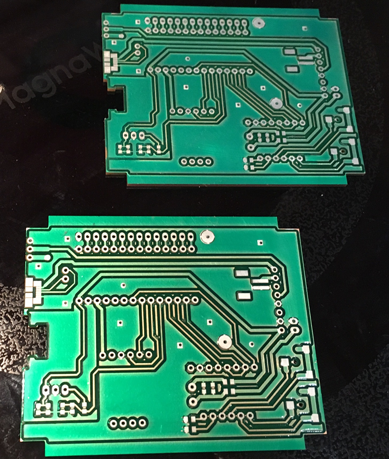
Pictured above is what my milled boards with film-type solder mask look like now. Milling these boards took about 25 minutes for the front side and about 15 minutes for the back. I can save 15 minutes if I turn off “use detail tool everywhere,” but I’d lose the thermal relief cuts on my ground pads. Applying the solder mask added about an hour to the entire process.
Here I’ll try to explain some of what I've learned about how to apply film-type solder mask like this to milled circuit boards. When written in detail, this sounds like a lot of work, but it goes very quickly, and my in-house prototype boards look nicer and are much more robust when done this way. While it’s true that adding film-type solder resist mask to a couple of prototype boards takes me about an hour end-to-end, most of that time is spent working on something else while I wait for UV exposure or for crosslinking.
Basics: Clean and Fixture
First, clean the board with Brasso metal polish and a paper towel to remove the anticorrosive coating before milling. Solder mask doesn’t bond well to the protective coating on the boards, and it's a lot messier to do this with Brasso after the holes have been drilled.
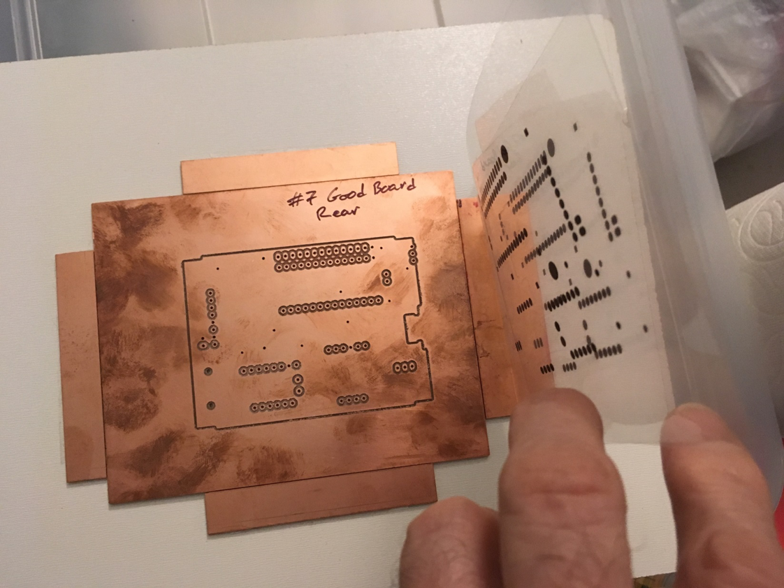
Alternatively, if you know the chemical composition of the protective coating on a particular brand of board, a liquid solvent could be used to remove it. In that case, do it after milling and just before applying the film. On the board below, you can see how quickly fingerprints and other signs of corrosion accumulate once the protective coating is gone.
For best results, I’ve found that the milling depth has to be set to 0.006" or less. The default board-milling depth of 0.008" is just barely too deep for the mask to adhere at the bottom of the valleys, especially if there are a lot of narrow traces close together. I’ve also found that milling at 0.008" makes thin traces and small pads noticeably more fragile when soldering or when plugging and unplugging a connector.
The board shown below was milled at the default depth of 0.008". It’s not too bad, but you can see that it might be hard for the film to get pressed down into some of the narrow valleys. That’s just one of the reasons that this was a failed “test board.”

To get away with a shallower milling depth, the board must lie flat on the bed with no warping. Warped boards can be straightened by carefully bending them in the reverse direction for a period of time, but the last thing I want is to be putting warped boards through a reverse warping process when I’m trying to finish a prototype. It’s better to avoid the warping in the first place.
One way to reduce warping issues is to use a gentler fixturing approach. Although Nitto tape is great for fixturing solids against significant milling forces, I’ve found that if you are going to be masking your boards, it is not necessary to use such a strong adhesive. With Nitto tape, PCBs nearly always get warped if you struggle to remove them. Even Scotch-brand “permanent” double-sided tape is too strong: To get the board loose, you have to pull and bend, and the second side of the board won’t be as flat as desired for milling at minimum depth.
[Note: Bantam Tools recommends using a small amount of isopropyl alcohol on Nitto tape to remove its adhesive quality so that boards can be lifted from the spoilboard of the machine without the risk of bending them.]
Fortunately, it’s not always necessary to use such strong adhesives when milling a PCB with the default settings on the Bantam Tools Desktop PCB Milling Machine. Even during cutouts, the shear forces applied to the board are easily handled within the adhesive strength envelope of Scotch-brand “temporary” double-sided tape applied across the entire surface of the board. I’ve found that if I’m careful during the removal process, I can mill one side of a board and remove it without any residual bend to affect the second side.
However, if a board already has curvature, temporary double-sided tape isn’t strong enough to pull it flat and keep it there, so stronger permanent tapes may be needed. I imagine that a vacuum table spoilboard would be an ideal approach to fixturing circuit boards: instant on, instant off, and no residues. For now, I use gentle tape fixturing. Here you can see typical warping of a PCB prior to milling.
Once the traces have been milled and the holes drilled on both sides of the board, I do one more thing before actually applying the mask: I place the milled board in an exposure frame and align the UV exposure mask to line up perfectly with all the solder pads and vias. I do the alignment before laminating on the film because it’s just a little easier to see things before the mask is applied. If you forget to do this, it’s no big deal — it’s more of a problem with the thicker coatings of paint-on or spin-coating mask, and it’s not really problem with the more transparent Dynamask adhesive film.
How to Make Exposure Masks
I use EAGLE for my board design. I used to export Gerbers for my masks, until I figured out this method that I prefer. Within EAGLE, I hide everything except the top or bottom “Stop layer.”

In the print dialog box, choose “Print to PDF.” Check the checkboxes so the patterned stop indicators will print as solid and black.

Step 1: Open in Illustrator.
When EAGLE has saved the PDF file, open that file in Adobe Illustrator, select all the spots as individual elements, and use “Transform Each” to change the size of each element to 115% of baseline in the X and Y directions without changing the spacing of the elements (as would happen if I transformed the entire thing or if I simply expanded it during the printing process).

Step 2: Print on laser printer.
From Illustrator, I print the page to a black-and-white laser printer at 100% size. Color laser printers don’t do a good job with black toner on transparencies. I bought a used black-and-white laser printer very inexpensively and use it exclusively for printing transparency masks. I print the page twice, once normally and once mirrored.
Choose an output paper type of letterhead to force the printer to use the manual feed tray, and then manually feed a high-temperature laser transparency. Don’t choose “transparency” as the paper type because most printers will reduce the temperature and the amount of toner too much on that setting, and the toner won’t be dense/dark enough. Don’t choose a heavyweight paper type because the printer will set the rollers too hot, and the transparency will warp and shrink unpredictably.
Sometimes the combination of printer and transparency leads to a little more shrinkage than can be tolerated, so the spots no longer cover all the pads at all corners of the PCB. If that happens, go back and print the pages again, but this time print the entire page at 101% of the original size. This will move all the spots slightly further apart, and they’ll once again match up with the pads and vias on the board.
Step 3: Line up the transparencies.
Put the two printed transparencies together with the toner sides touching, which doubles the density of the spots. Lay the two over the board and cut the excess transparency material off so that the mask will not protrude over the edges of the PCB. This is important when it comes to keeping the transparency perfectly flat during exposure.
I cut a little extra off the top edge of the top layer of transparency to make it shorter than the lower layer. That way when I get the two copies perfectly lined up, I can just use a strip of Scotch tape to hinge them together in perfect alignment. Don’t tape down multiple edges, or you may get buckling at a later step. Just one piece of tape as a hinge at the top will be fine.
Do the same thing again for the bottom layer of the board. Once I have self-aligned and taped together the two copies of each layer and cut them to a size that will fit on the board blank, I’m ready to put each one into a transparency exposure frame and secure their alignment with the board itself.
Step 4: Set up the exposure frames.
The exposure frames I use are just flat pieces of coated MDF, each one a little bit larger than the PCB. I paid about $10 for a 24"x48" slab, and I used my track saw to make a lifetime supply of frame bases in about an hour. The local home improvement shop will slice it up for you for $1.00 per cut, so you pay about $6 more if you don’t like to saw things up yourself.
The PCB is held in a fixed location on the frame by four scraps of PCB material that are pushed firmly up against the board and are attached to the frame with glue or double-stick tape. The scraps have to have at least one straight edge, and they need to be the same thickness as the board they’ll secure. The board itself is not taped down — it just drops in and is held in place by friction.
Here you can see exactly how the frame is made from scraps to secure the board in place. You can also see that the two layers of transparency are only secured along one edge, to prevent buckling under vacuum.
With the milled PCB in its frame, I position my exposure mask over the board, and when I’m satisfied with the alignment, I anchor it with a hinge of Scotch tape across the top. The mask should be hinged, not to the MDF frame backing, but to the scrap of PCB that keeps the board locked into its location. This way the exposure transparency will lie perfectly flat during the exposure process.
Once the mask has been hinged at the top, it’ll stay in position, and the alignment will be correct no matter how many times the board is taken in and out. Don’t put Scotch tape or packing tape over the area where the mask will be applied, because some tape can absorb a lot of UV, and you may prevent curing in the areas that are covered.
You can see two pieces of Scotch tape here: one is holding the upper layer of transparency in alignment with the lower layer, and the other is hinging the upper layer (both layers, really) into “perfect” registration with the board.
I align exposure transparency frames for both the front and back of the board before I apply the solder mask film. When the mask has been applied, the board will drop back in, and the alignment will still be correct.

Step 5: Apply the Dynamask.
At this point, I remove the board from the frame and proceed to apply the Dynamask, a uniform-thickness film of UV-sensitive solder resist that’s also a hot-melt adhesive. It’s supplied with a protective coating on each side: one of the protective coatings is a stretchy matte plastic and the other side is clear Mylar.
The matte side is removed in order to apply the Dynamask to the board, and the clear side is only removed after exposure, when it’s time to “develop” the exposed board. To remove the matte side covering on the Dynamask, use two small pieces of clear packing tape, one on each side of the film. Scotch tape is not sticky enough. Getting this initial coating off can be extremely difficult and frustrating at first, but sooner or later, you get the knack and it “magically” becomes much easier.
Cut a piece of Dynamask that will cover all of the milled portion of your PCB and a little larger but is small enough to fit completely within the uncut board. Peel down only a thin strip of the protective matte covering across the top of your piece of Dynamask, to expose the adhesive.
Position the Dynamask so it covers the entire milled portion of your board and extends a small distance past the final cutout outline. Use your fingers to smooth out and press down the thin strip of exposed adhesive to anchor it firmly. Try to make sure that the strip you press down with your fingers is outside the final milling outline, because there may be bubbles along that edge no matter how hard you press it down. Peel away the remainder of the matte coating, but don’t let the adhesive mask touch the board or anything else.
Step 6: Run through laminating machine.
Feed the board and attached mask into the rollers of a hot laminating machine while keeping tension on the mask, so the mask only touches the board when forced to by the rollers. This will generally prevent bubbles and wrinkles. You have to get your fingers right up close to the rollers at the end, so the rollers have to be uncovered for this to work.
If you drop the mask film too early or release the tension on it too much at any point in the process, you will almost certainly get wrinkles. The mask will still work so long as the wrinkles don’t go right across surface mount pads, but it won’t be as pretty. Commercial film applicator systems have rolls of film both above and below the board, and tensioning systems ensure that both sides get applied perfectly in a single pass. I’m sure it would be possible to build a home jig for this, or perhaps someday there will be a machine to do it for us.

Tips on Laminating
Some internet tutorials (including one made by the primary eBay vendor of Dynamask) tell you to turn up the heat all the way and to run the board through multiple times. This will only work if your machine is naturally underpowered and goes too fast, so it has trouble heating the board and melting the adhesive. If that’s your laminator, then you have to work hard to get good adhesion, and you’ll very likely see wrinkles. It’s better if your machine can heat the board to the right temperature in a single pass.
The inexpensive-when-new four-roller laminators that have only one speed and heat only one roller can definitely be made to work well, but only by modifying the roller speed (to make it slower) and adjusting/calibrating the thermostat. I’ve done this in the past, but I wouldn’t recommend it.
Do not make the laminating machine too hot, or you will get wrinkles; 125°C is perfect.
Do not run your board through more than once, and don’t reverse it while it's running through. When the adhesive is hot, it gets slippery: the clear Mylar cover may slip, and Dynamask will get all over the rollers. Even if that doesn't happen, you will get wrinkles.
This is what the board looks like when the temperature is too high. These wrinkles were caused by running the board through the laminating rollers twice, and at too high a heat. It was the last piece of Dynamask from my first order, and nobody was supposed to see it, so I built the prototype board anyway.

The ideal laminating machine has six silicone rollers, speed control, and temperature control. Models with those features can be from $500 – $2000 new, but they often come off commercial leasing packages and typically look a little shopworn, so they’re nearly always available on eBay for around $100. My favorite is the popular Sky 335R6 laminator; I bought two of these from different sellers for $85 each.

I apply Dynamask (and other adhesive films) at 125°C with a speed setting of 2, and I never get wrinkles unless I accidentally drop the film too soon or pull on it very unevenly.

When the board comes out of the rollers hot with Dynamask, run it under cold water to cool it quickly. I was skeptical of this advice but have found that it really does seem to improve bonding. Pat the board dry, set it back in the exposure frame, flip down the exposure mask, and check that it still lines up correctly with all the solder pads and vias.
Exposing the Board
I use a 15-watt, 18-inch-long single-bulb black light lamp. I got a pre-packaged black light including the bulb for $24 at a local home-improvement center. I also have a fancy exposure unit that I use for exposing silkscreen emulsions, but this basic black light is much easier to use for exposing PCBs the way I do it.
The bulb alone costs $18, so it was an easy decision to get the prebuilt lamp for $24.

I also use a small homemade vacuum frame to hold everything in perfect alignment during exposure. I have a “proper” vacuum frame that I use for other purposes, but for making boards, I prefer the very small and simple setup that I’ll describe here.
Step 7: Make the vacuum frame.
The vacuum frame is simply made from a gallon-size freezer bag:
Tape a small washcloth over a piece of MDF that’s just slightly smaller than the opening of the freezer bag.
Slide the MDF with washcloth into the freezer bag, then poke a small hole in the bottom of the bag and force a length of plastic tubing through the hole. I try to keep this a tight fit, but if the hole gets to be too large, you can simply tape it up with clear packing tape.
Tape the end of the plastic tubing on top of or under the washcloth.
The washcloth serves as a porous surface, so that when I apply suction, the air will have an easy path to get to the tubing and be sucked out.
Here’s the underside of the MDF baseplate with a washcloth taped onto it, quick and dirty.

The plastic tubing I bought had a permanent curve that didn’t relax even with heat, so I taped it to a popsicle stick.
The red stain is from the application of a red liquid solder mask to an etched PCB earlier. It didn’t work well for milled boards because too much of the mask accumulated down in the milled isolations between traces. If we could mill off just the copper and leave the FR-1 resin intact, we could use liquid resist just like on any other board.

Step 8: Turn on suction.
When it comes time to do the UV exposure, slide the transparency alignment frame into the bag and position it on top of the washcloth, zip the bag closed, and turn on suction.
I’m using a fairly quiet suction pump that I use for de-bubbling castings. When you turn on suction, you have to be quick to smooth out any wrinkles in the plastic bag before the suction locks them in place. You don’t need a dedicated vacuum pump—I’ve done this successfully using an ordinary vacuum cleaner for suction.
Here’s the quick-n-dirty vacuum frame with vacuum applied. There’s no mask material on this board, so you can see the alignment clearly. When exposing, the more closely the transparency is pressed against the solder mask, the cleaner and crisper the mask openings will be. It’s much easier to get crisp outlines with the vacuum. It can be done with weights and sheets of glass, but it’s easier just to throw together a vacuum frame.

Step 9: Turn on black light.
Check one more time to be sure the black spots still line up perfectly with the pads and vias. Prop the black light up about 3” above the board and turn it on. If you calculate the fluence, you’ll get an answer suggesting that only 45 seconds of exposure should be needed, but this isn’t correct. That’s because plastic absorbs UV light, and there are now four layers of plastic between the black light and the board: one layer of freezer bag, two layers of laser transparency, and one layer of protective coating still on the Dynamask.
With this setup, I’ve found that a 5-minute exposure using a 15-watt black light bulb positioned 2.5”–3” above the PCB gives perfect results.

If you accidentally leave the light on too long, some of it will get through the black spots, and your solder mask will stick to the pads as well as to the rest of the board. If it sticks too hard, you’ll have to use a fiberglass pen or a spot-sanding rig to get it off. I use an old darkroom exposure timer to turn off the black light automatically, so even though I’m forgetful, I don’t ruin boards this way anymore.
Step 10: Wait 20 minutes.
After the exposure is done comes the hardest part of this entire process: Cover the board and let it sit in the dark for 20 minutes so the UV-triggered polymerization can proceed, and the mask material can harden. In a pinch, you can get away without waiting, but if you don’t wait, the mask will still be soft when you apply the developer, and you’ll risk washing away parts of the mask that you wanted to keep.
Some published material says that you should wait 24 hours for polymerization to complete. I tried that but didn’t see any difference. Perhaps it would make a difference with specific production techniques, but 20 minutes has worked very well for my prototype boards.
Step 11: Peel off protective coating.
Now take the board and carefully peel away the clear protective coating. Don’t touch the dry bare mask yet, as it’s not yet fully cured. Touching it with your fingers or a glove at this stage will make it come out with fingerprints, or with a matte finish rather than the normal gloss finish.
If any of the UV-exposed parts of the mask peel away from the board when you take off the protective Mylar coating, the bond is not good, and the remainder will eventually begin to chip and flake as you work with the board. If I were to see that the mask wasn’t adhering properly, I would put the board into a 5% sodium hydroxide (caustic soda) stripping bath, remove all the mask, and start over.
Poor bonding most often comes from failing to remove the anticorrosion coating from the board or from oils or other contaminants on the surface, but it can also come from insufficient heat and/or insufficient pressure during the application of the mask, or insufficient UV exposure or cure time. Each of those things has happened to me, when I was trying to figure out which steps matter and which do not.
If the mask is glued to the board properly, it won’t peel away with the Mylar, and you’re ready to “develop” the mask.
Step 12: Scrub with sodium carbonate.
Pour into a plastic food container about a cup of water (about 250 cc) and half a teaspoon (2.5 grams) of sodium carbonate powder. Place the board into the solution.
Get a fairly soft brush (I use an acid brush, or in a pinch I’ll borrow one of my wife’s paintbrushes) and begin brushing over all the places where the mask was protected from the UV light. If the exposure was correct, you’ll see the mask dissolving to expose bright copper at all the pads and vias.
If you don’t get sharp margins around your pads within a minute or so, it means that a little light leakage got through and hardened up the mask under the black spots. In this case, use a stiffer-bristle brush, such as a toothbrush, to remove the mask in those locations.
Make a note, and next time, either print your spots darker or reduce the exposure time a little bit. When you’re done with the developer bath, the pads shouldn’t have even the faintest tint of green left on them, because even a very thin coating will prevent you from soldering to those pads. Rinse well after developing. A sponge can help to make sure the developer is gone from all the nooks and crannies.
If you scrub and scrub, and the green stuff won’t really come off at all, it probably means you forgot to take off the protective Mylar coating. You’re not the only person to have done this. You’re not even the only person to have done it more than once.
When you put granular sodium carbonate in water, it makes carbonic acid and sodium hydroxide. The recommended developer solution is given as 10 grams per liter (1% wt/vol) at 45°C, but I’ve found that it doesn’t make a lot of difference if you mix the sodium carbonate a little too strong or too weak, and it doesn’t make a lot of difference whether the water is room temperature or bath temperature. If you get it perfectly right, the masked spots dissolve with minimal brushing, but if the solution is too weak or too cold, then you just end up using the brush for an extra 30 seconds. The solution can be reused until it gets slimy from all the solder mask you’ve put into it.
Remember that sodium carbonate is washing soda, not baking soda, but the two are related: if you need sodium carbonate when all the stores are closed, you can make some by putting baking soda in the oven at 400°F for an hour or two, until it has lost about 20% of its weight. If you do this, don’t use an aluminum dish.
Step 13: Expose to UV.
After developing and rinsing the board, dry it gently and put it under the UV light for another 15 minutes to harden up. Some people suggest placing it in an oven at 100°Celsius for 5 minutes, but I haven’t found that to make a difference.
Step 14: Repeat for opposite side.
Now that one side of the board is successfully masked and the mask is cured reasonably hard, I repeat the whole process for the opposite side.
Step 15: Mill the board.
I find that it's best to mill the final board outline after the solder resist has been solidly bonded to the board. The main reason is that when laminating film to the board, you can’t let the film go beyond the edges of the board or it will stick to the laminating rollers and create a real mess.
It’s much easier to mill the traces and holes for both sides, then apply and cure the top mask, then apply and cure the bottom mask, then silkscreen any desired labeling, and mill the outline at the very end. The Bantam Tools Desktop PCB Milling Machine locating bracket makes this very easy to accomplish.
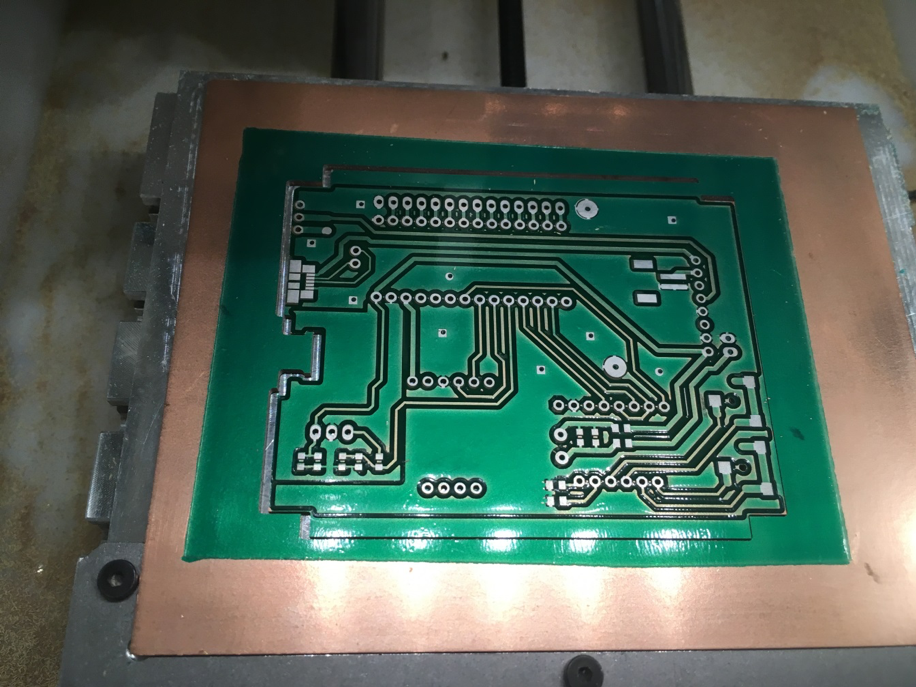
Here the fully masked board has been put back into the mill, and the cutout has been milled.
I plate most of my boards with some other metal over the bare copper. Sometimes people ask me why I bother, since they don’t plate their boards and they don’t have any problems. The answer is that I live in Honolulu, where humid salt air means that unprotected copper traces can corrode away in a matter of days. If I’m not soldering the board immediately (or if there are any optional pads or headers), then I always plate it with tin or gold as soon as both sides have been masked.

Thanks for sharing your knowledge and technique, Dr. Feied!
If you use this technique, show us your results! And if you have a useful tip or trick, let us know so we can share with the community! Feel free to reach out anytime via support@bantamtools or by tagging us on your social posts with #bantamtools and @bantamtools.